Aluminum Nitride Model Explains Radiation-Induced Semiconductor Burnout
A model links local electric-field strength to single-event burnout in aluminum nitride diodes, offering a basis for comparing materials and device designs.

For electronics exposed to energetic particles, a device’s voltage rating alone may not describe its risk of catastrophic failure. A theoretical model developed by researchers at North Carolina State University links single-event burnout (SEB) to the intense electric field created along an ion’s path through a semiconductor. The work uses aluminum nitride (AlN) diodes to explain how that local field can trigger a destructive failure.

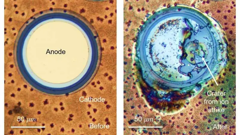
How one particle can destroy a diode
SEB occurs when one energetic particle causes damage in an electronic device operating at high voltage. In the researchers’ account, a heavy ion passing through a semiconductor generates charged particles along its track. When an electric field is applied across the diode, positive and negative charges separate. That charge separation creates a concentrated field in the region traversed by the ion.

If the local field becomes strong enough, it can initiate an electron avalanche. The resulting rapid release of energy can inflict catastrophic physical damage, leaving the device unusable. The failure therefore depends on a chain of events: an ion deposits charge, the applied field separates that charge, the field intensifies locally, and an avalanche releases enough energy to damage the structure.

That sequence helps explain why SEB has been difficult to assess from applied voltage alone. Engineers have measured the maximum voltage at which failure may occur, but voltage does not by itself capture the field inside a particular device. The relevant field depends on how the material and device structure respond to the applied voltage and to the charge created by the particle.
Why the field matters for material comparisons
The study examines AlN, an ultrawide-bandgap semiconductor that can operate under high electric fields. Researchers irradiated AlN diodes with heavy ions and combined their experimental data with information from other semiconductors and computer simulations to build a mathematical description of SEB.

The model indicates that AlN can withstand substantially larger electric fields before SEB occurs than some other semiconductors considered in the work. That comparison is framed in terms of electric-field strength rather than applied voltage. For engineers weighing semiconductor materials, this is the more useful basis: the same voltage can produce different field conditions depending on the device and material.

The distinction also changes how a failure threshold should be interpreted. A measured voltage marks the behavior of a specific device under its test conditions; a field-based comparison aims to describe the material response more directly. The reported model connects those views by relating the local field around an ion track to the onset of an avalanche and subsequent damage.
What the model offers device designers
The practical value is a physical framework for investigating how radiation tolerance might be improved. If a design can reduce the local field concentration or otherwise prevent the conditions that lead to an avalanche, it may reduce the likelihood of SEB. The researchers describe the model as applicable to different devices and semiconductors, drawing on their AlN experiments alongside data for other materials and simulations.
That does not establish a finished design recipe or a universal safe operating limit. The report provides no numerical field thresholds, ion species or energies, test fluence, device geometry, or detailed design changes. Engineers would still need test conditions and device-specific data before translating the mechanism into qualification limits or layout decisions. The model’s contribution is to identify the local electric field as a key quantity for that work.
AlN’s ability to endure larger fields before burnout makes it a material of interest for high-power and high-radiation environments. The researchers point to potential relevance in space missions, nuclear power stations, fusion reactors, and medical devices. Those are application areas where electronics may face energetic particles, but the study does not report a qualified product or demonstrate operation in each setting.
A basis for radiation-tolerant electronics
For teams developing electronics for extreme environments, the central takeaway is that radiation tolerance involves more than selecting a semiconductor with a high nominal voltage capability. A particle can create a concentrated, transient field inside the device, and that local condition may determine whether an avalanche develops. Material properties and device design therefore have to be considered together.
By tying SEB to the field formed along an ion’s path, the North Carolina State University researchers offer a way to compare semiconductor behavior and guide further design studies. The next useful step is to connect that framework to specific device structures and clearly reported irradiation conditions. Until those details are available, the model explains a failure mechanism and points toward design criteria; it does not supply a ready-made operating limit.
 AMD Venice Uses 2.5D Packaging to Feed More Bandwidth Into EPYC Zen 6
 CNC Controller Board Design: Interfaces, PCB Specs and Assembly Testing
 Stratasys and Nano Dimension End $42.5 Million Markforged Sale Agreement