AMD Venice Uses 2.5D Packaging to Feed More Bandwidth Into EPYC Zen 6
Venice pairs 2.5D packaging with split I/O dies to support 1.6 TB/s of chiplet bandwidth, while SP7 and SP8 target different system needs.

AMD’s Venice server processors put data movement at the center of their design. The move to 2.5D packaging supports a stated 1.6 TB/s of bandwidth between compute chiplets and I/O, while two I/O dies provide the perimeter and fabric layout needed to connect them. Those choices shape the rest of the system: SP7 and SP8 use different I/O designs, and the 12-core and 32-core compute chiplets are built around different bandwidth demands.
Mahesh Subramony, AMD’s corporate vice president of design engineering and leader of its server architecture team, described these decisions in a discussion of the Venice SoC. His account makes clear that packaging, memory configuration, core count and cache behavior are linked design problems. The chiplets have to move enough data to keep their cores productive, but doing so also affects die area, power and the cost of the finished processor.
Why Venice moves to 2.5D packaging
The previous generation moved just under 700 GB/s between its compute chiplets, or CCDs, and the I/O die. Conventional packaging and GMI links were suitable for that bandwidth, Subramony said. Venice raises the figure to 1.6 TB/s, with each CCD provisioned to drive data into the I/O die.
AMD estimated that carrying this volume of traffic through conventional packaging would consume roughly 10–15% of the SoC’s total power budget. That estimate concerns the energy spent transporting bits across the package; Subramony said it applied regardless of the picojoules-per-bit figures reported in technical papers. A shorter, denser die-to-die connection offered a way to provide the bandwidth with lower power and latency.
That connection also places stricter demands on physical layout. The CCDs and I/O die need to meet across short-reach links, with compatible interface widths and very little distance between them. Previous designs could route connections over longer paths through the package, which gave the dies more freedom in their dimensions and placement.
In Venice, the I/O die needs enough edge length for its external I/O and enough connection area, described by Subramony as “beachfront,” for the CCD links. Splitting the I/O function across two dies gave the design the perimeter needed to place those connections close to the compute chiplets. The short, low-power links also kept the extra die boundary from imposing a major power or latency cost, he said.
One I/O design, used twice
AMD used the same I/O die design twice in the package, rotating one copy by 180 degrees. That mirrored arrangement avoids designing two different dies for the pair, but it duplicates some circuitry. Blocks that need to exist only once for the full SoC, including the root of trust and some boot-related I/O, are present on both copies and add area.
The other challenge is making the two dies work as one fabric. They can be viewed as separate domains, but Venice must also support an NPS1 configuration in which the SoC operates as a single domain. AMD had to ensure that the mirrored topology could provide the required quality of service, bandwidth and latency when both I/O dies work together.
Subramony sees tiled designs becoming more useful as SoCs grow to higher core counts. Dividing functions among tiles can help solve the physical problem of fitting connections around increasingly large compute designs, though it brings fabric and system-level challenges that designers must address.
SP7 and SP8 serve different system targets
Venice’s SP7 and SP8 platforms both use two I/O dies, but AMD designed distinct I/O dies for the two sockets. SP7 emphasizes compute and memory bandwidth. SP8 targets a different balance: lower compute requirements, a large number of I/O lanes and cost control.
A single superset die could have covered both platforms, but it would have carried features that one or the other did not need, adding cost to both implementations. AMD instead tailored each design to its intended configuration. SP7’s I/O die supports more compute, fewer I/O lanes and more memory channels. SP8 has half as many memory channels and provides all 128 PCIe lanes per socket, while targeting up to 96 Zen 6 cores or 128 Zen 6c cores.
The distinction is more than a matter of scaling one design down. Memory channels, I/O lanes and compute capacity compete for die area and influence how the package connects to the rest of a server. Separate I/O designs let AMD allocate those resources according to each platform’s requirements, rather than making both carry the cost of a shared set of capabilities.
CCD links follow bandwidth needs
The number of links from a CCD to the I/O die also varies with the workload each design is meant to serve. The 32-core CCD has four SDP ports, following a rough rule of one port per eight cores. AMD sized those links so the cores can draw the bandwidth needed for their performance and instructions-per-clock targets.
The 12-core CCD has three SDP ports, a high count relative to its core total. Its intended pairing with MRDIMMs helps explain the choice: each CCD needs to contribute enough bandwidth to help saturate 16 memory channels of 12,800 MT/s MRDIMMs. Looking only at bandwidth per core can make three links appear excessive, but the relevant target is the memory bandwidth available to the full SoC.
A spare core helps recover large CCDs
The 32-core CCD physically contains 33 cores, along with 33 L3 cache slices. It will always expose 32 active cores; AMD does not plan a 33-core product. The extra core gives the company the option to disable a defective core and its associated cache slice while retaining a functional 32-core chiplet.
That arrangement requires the mesh to remain intact after one core and slice are harvested. AMD designed the architecture to support that choice, while keeping the active core count fixed. Subramony said the added core was possible to fit during design and reflected a cost consideration: larger dies on advanced process nodes are expensive, and recovering a die with one defective core can help yield at volume.
Larger L3 trades lookup time for more hits
The 12-core and 32-core CCDs differ in L3 capacity and mesh size, and that changes cache lookup latency. On the 32-core design, checking the 128 MB L3 takes a few extra clock cycles before a request proceeds farther out. AMD can explore speculative techniques to hide some of that delay, but the larger cache still adds lookup time. Beyond the cache, Subramony said, the path from fabric to memory is almost identical.
A controlled measurement on an otherwise idle processor, using a closed-page load from DRAM, should expose a latency difference between the CCDs, largely because of the extra L3 lookup time. That result does not by itself describe how a workload performs. A larger cache can increase the number of requests served without going to memory, especially when more threads are resident on a CCD. Those hits can offset the lookup penalty in workloads that benefit from the additional capacity.
Why dense CCDs are not the first target for more stacked cache
AMD’s 96-core offering pairs a 12-core CCD with X3D technology, adding another 96 MB of L3 for about 144 MB per CCD. Subramony said the tradeoff looks different on a denser CCD: when fewer cores are active, the existing L3 is shared among them, increasing the effective cache capacity per active core.
Adding a large stacked cache to the dense design would raise cost, and AMD would need to weigh that against the performance gained. The 256-core part is aimed at balanced throughput under a tight per-core power budget. For that product, Subramony said, AMD would first consider ways to provide more bandwidth or frequency rather than adding a large X3D die.
That choice captures the broader Venice design approach: the best answer depends on where a platform’s limits sit. More cores call for enough chiplet bandwidth; memory-heavy configurations need links that can feed many channels; and larger caches trade lookup time and die cost for more local hits. Venice’s split I/O and platform-specific dies give AMD room to make those tradeoffs differently across SP7 and SP8.
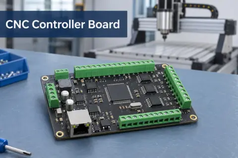 CNC Controller Board Design: Interfaces, PCB Specs and Assembly Testing
 Stratasys and Nano Dimension End $42.5 Million Markforged Sale Agreement
 Xometry Q3 2026 Revenue Reaches $252.4 Million as Marketplace Margins Rise