22-Layer HDI PCB Design: Stackup, Via Geometry and Impedance Constraints
A 22-layer HDI board’s feasibility depends on checking its stackup, buried-via geometry, material choices and impedance requirements together.

Feasibility starts with the complete construction
A 22-layer HDI PCB can fit dense BGA routing, high-speed signals and several power domains into a fixed board outline. The harder question is whether the specified vias, copper, dielectrics, impedance and finished thickness can all coexist in one manufacturable stackup. A design calling for 0.10 mm microvias, deep buried vias, ±10% impedance tolerance and a fixed nominal thickness needs a construction review before anyone can confirm that the layout can remain unchanged.

That review must consider the finished board as a system. Via spans affect drilling depth and routing access; dielectric thickness affects both impedance and via geometry; copper thickness affects trace etching; and the material construction determines electrical and mechanical behavior. Checking each number in isolation can miss conflicts between them.
HDI construction is useful when BGA escape routing or signal transitions cannot be managed efficiently with conventional through-holes. It adds laser-drilled microvias, blind or buried connections, and sometimes via-in-pad structures. High-speed computing and FPGA boards, networking equipment, industrial VME processor cards, medical instrumentation and aerospace electronics are among the applications described for this class of board. A 22-layer design does not automatically require HDI: conventional multilayer fabrication can suffice when through-hole routing leaves enough space.
Layer assignment and thickness
One example symmetric layer plan pairs the outer layers L1 and L22 for signals and BGA breakout. L2 and L21 serve as ground references; L3 and L20 as high-speed signal layers; L4 and L19 as ground; L5 and L18 as internal signal; L6 and L17 as power distribution; L7 and L16 as ground; L8 and L15 as internal signal; L9 and L14 as ground; L10 and L13 as high-speed signal; and L11 and L12 as central ground references.
In that arrangement, L3 and L20 can carry controlled-impedance stripline signals, while L10 and L13 offer additional high-speed routing channels. Critical signal layers need suitable reference planes so return current has a continuous path. The remaining signal layers can support BGA fanout and internal connections.
This functional plan is only a starting point. A fabrication-ready stackup must specify the actual core and prepreg constructions, dielectric spacing, finished copper weights, impedance geometry and lamination balance. The copper and dielectric layers must fit the mechanical thickness requirement together. For a 2.25 mm nominal finished thickness, changing dielectric spacing to tune impedance can also change drilling geometry and the overall stackup, so it cannot be treated as an independent adjustment.
Choosing the HDI buildup and via spans
A 1+20+1 construction has a 20-layer central structure with one HDI buildup layer on each side. L1–L2 microvias connect top-side pads or traces to the adjacent layer; L21–L22 microvias provide corresponding bottom-side access. Buried vias connect selected internal layers, while plated through-holes can connect L1 to L22 when a full-depth path is needed.
Where a signal microvia lands on a ground-reference layer, its capture pad needs clearance from surrounding ground copper and a connection to the intended signal network. The layer transition, pad, antipad and reference change all affect the finished interconnect.
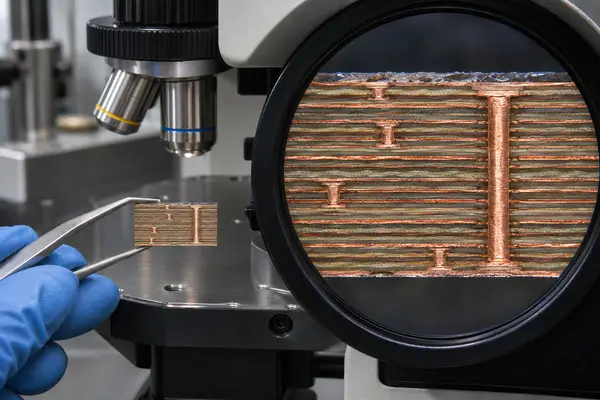
A 2+18+2 structure adds buildup connections for denser routing, at the cost of more sequential lamination and microvia processing. The choice depends on BGA escape needs, the number of required layer transitions and reliability requirements. Extra buildup levels are useful when they resolve a specific routing constraint; otherwise, they add process steps without solving a demonstrated problem.
Via dimensions need to be assessed against the actual dielectric or board depth. For example, a 0.10 mm laser-entry diameter through 0.075 mm of dielectric gives a nominal depth-to-diameter ratio of 0.75:1. Whether that microvia is practical also depends on capture-pad dimensions, drilling geometry and metallization.
Filled and capped microvias can be placed in BGA pads to route beneath fine-pitch components. Copper fill, planarization and capping must leave a flat, solderable surface. Voids or uneven caps can affect solder-joint quality.
Deep mechanical buried vias present a different constraint. For an L2–L21 connection with an approximately 2.0 mm drilling depth, a 0.20 mm drill gives a 10:1 aspect ratio; a 0.25 mm drill gives 8:1. Those ratios assume the stated dimensions are drill diameters. If they instead describe finished holes, drill size and aspect ratio need to be recalculated. High aspect ratios make uniform barrel plating more difficult, so hole-wall preparation and copper continuity must be assessed using the actual depth.
Full-depth through-holes can consume routing space across the entire stackup. Unused via barrel sections on high-speed nets can also form stubs, making antipad design or backdrilling relevant to the signal path.
Example project constraints
The source’s demanding project example specifies 22 layers and a 228.35 × 160 mm outline, with 1+20+1 HDI construction and a finished thickness of 2.25 mm ±10%. It calls for 0.10 mm laser microvias on L1–L2 and L21–L22; 0.20 or 0.25 mm mechanical buried vias on L2–L21; and 0.25 mm plated through-holes.
Other listed requirements are minimum trace and spacing of 85/100 µm, BGA pitch of 0.8/1.0 mm, 17 µm inner signal copper, 35 µm copper on selected power planes, and 17 µm base outer copper with approximately 32 µm finished. The specified controlled impedances are 40/50Ω single-ended and 80/100Ω differential, each with ±10% tolerance. The named interfaces are SerDes up to 6.25 Gb/s and DDR3; the stated finish is ENIG.

These figures describe an example project, not a guarantee that every fabricator can meet them. Three constraints deserve early attention. First, the thickness tolerance surrounds the approved 2.25 mm nominal construction; it does not itself permit an unapproved change to that nominal. Second, 85 µm traces must be evaluated using finished copper geometry, with etching compensation that may differ between internal and outer layers. Third, a 40Ω target at ±10% allows ±4Ω deviation, so the fabricator’s capability and coupon method need to be agreed.
Industrial boards can add connector-hole requirements. The example cites a VME board with 105 holes at 0.60 mm and 320 holes at 1.00 mm. Such press-fit features need connector-specific finished-hole tolerances, plating details and compatibility with board thickness. ENIG on BGA pads does not by itself define the finish inside press-fit holes.
Impedance, signal loss and material selection
Controlled impedance depends on finished trace width and thickness, differential spacing, dielectric thickness and properties, and the continuity of reference planes. Calculations should use the etched conductor dimensions rather than only the nominal CAD geometry. Transitions also need review: capture pads, antipads, via barrels and unused stubs can introduce reflections.
For a 100Ω differential pair at ±10%, the acceptable measured range is 90–110Ω. At 6.25 Gb/s NRZ, the Nyquist frequency is approximately 3.125 GHz, while higher-frequency signal components also affect channel performance. Dielectric loss, copper roughness, channel length and connector transitions therefore matter alongside the impedance target. DDR3 routing also needs suitable clock and data-strobe relationships, timing margin and termination.
Coupon measurements verify selected fabricated transmission-line structures; they do not establish the performance of every complete channel. Full-channel behavior still needs electrical simulation or system-level validation. The coupon design and measurement conditions should be agreed as part of the build requirements.
Material choice must account for dielectric properties at relevant frequencies, available core and prepreg thicknesses, thermal behavior and compatibility with the HDI process. The source lists several examples, with manufacturer data tied to specific constructions and test conditions:
Isola I-Tera MT40: A published 0.051 mm core construction has Dk 3.30 and Df 0.0026 at 10 GHz. Other constructions have different values.

Panasonic MEGTRON 6: Panasonic lists Dk 3.34 and Df 0.0037 at 13 GHz for R-5775(N); other variants differ.
Shengyi S7439: Shengyi lists Dk 3.80 and Df 0.0068 at 10 GHz using the specified IPC test method.
ITEQ IT-968G: For a specified 55% resin-content construction, ITEQ lists Dk 3.59 and Df 0.0050 at 10 GHz.
TUC TU-862HF: Published data for a specified 50% resin-content construction gives Dk 4.4 and Df 0.010 at 1 GHz. Because that measurement uses a different frequency from the figures above, the values should not be compared directly. TU-862HF is not an automatic electrical substitute for I-Tera MT40 or MEGTRON 6.
A material substitution can preserve an existing layout only if the replacement meets the approved electrical and mechanical requirements. The stackup needs to be recalculated using available core and prepreg constructions; impedance must be checked on every controlled layer; and channel loss, lamination behavior, thermal expansion and dimensional stability need evaluation. Any allowed conductor compensation must also be confirmed. Similar nominal Dk values do not establish equivalent impedance, insertion loss or manufacturing behavior. A substitution affecting the approved construction requires customer approval.
Fabrication controls and verification
For a typical 1+20+1 board, fabrication begins with imaging, etching and automated optical inspection of inner layers. Buried vias are drilled, desmeared, metallized and plated before later lamination makes them inaccessible. The 20-layer central structure is then aligned and laminated; outer dielectric and copper buildup layers are added, followed by laser drilling and the specified microvia metallization, filling and capping. Final processing can include through-hole plating, outer-layer circuits, solder mask, ENIG and profiling.
Several process risks follow directly from this sequence. Material movement during lamination can shift internal features and reduce alignment between buried vias and capture pads. Material-specific dimensional compensation, controlled lamination and registration inspection help manage that risk. Deep holes can suffer nonuniform barrel copper or plating discontinuities; drilling, desmear and plating must suit the actual depth, with microsections used to examine continuity.
Microvia reliability depends on laser drilling, target-pad preparation, copper deposition, fill and cap quality. Fine-line impedance can shift with etching variation or uneven finished copper. Copper-dependent etching compensation, trace measurement and representative impedance coupons address those dimensions. Copper balance and dielectric construction also affect warpage and thickness variation, so stackup balance, lamination control and finished-board inspection matter. Connector holes need dimensional inspection against the specified finished-hole and plating requirements.
Quality records may include electrical testing for opens and shorts, microsections of buried vias and microvia interfaces, layer-registration and fill inspection, impedance coupon measurements, and dimensional checks of thickness, outline and connector holes. Thermal reliability testing can be specified where required. Inner-layer optical inspection catches conductor defects before lamination. The applicable IPC-6012 performance class and project requirements set acceptance criteria; required records and reports should be settled before fabrication.
Prototype planning, schedule and cost
A prototype should verify a construction that can carry into production. Even a 3–4-piece order may require substantial engineering preparation when it combines deep buried vias, filled microvias and tight mechanical requirements. Before release, confirm materials, dielectric spacing, copper weights, layer assignments, via spans and fill requirements, controlled impedance and tolerances, mechanical dimensions, and acceptance tests. Keeping the intended production construction during prototyping can reduce the chance of later qualification work or redesign.
Lead time depends on laminate availability, sequential lamination, laser drilling, microvia filling and capping, buried-via processing, resolution of stackup or mechanical conflicts, and the required testing. Complete fabrication data and approved alternate materials can reduce avoidable delay, but the number of boards alone does not determine schedule: a four-piece order may still need the same critical process stages as a larger batch. Delivery timing needs confirmation after review of the construction, materials and capacity.
Cost likewise reflects the buildup count, deep buried holes, filled or capped microvias, low-loss materials, fine-line tolerances, inspection and quantity. If the routing permits, a 1+20+1 construction may cost less than a higher-order buildup. Other options include omitting via filling where it has no electrical or assembly purpose, reviewing noncritical tolerances, and considering approved materials already available for manufacture. Each change must preserve electrical performance, mechanical fit and interconnect reliability.
Release details that prevent avoidable problems
Before fabrication data is exchanged, a non-disclosure agreement can be requested and file-handling terms agreed. IPC Class 3 is not an automatic requirement for every 22-layer board; the applicable class follows intended use and contractual reliability needs. Serial marking, traceability records, special packaging and a certificate of conformity can be specified in the order requirements.
Gerber files, drill drawings, stackup and fabrication notes need to refer to one approved revision. Any discrepancy should be resolved before work begins. Customer-supplied laminate can be evaluated for identity, condition, traceability, dimensions and process compatibility. Combining different designs on a panel may work when materials, thickness, copper and processing are compatible; different HDI constructions can prevent it.
Surface finish selection should reflect component terminations, assembly process, storage period, flatness and reliability requirements. Edge plating and castellated features may be possible, but their geometry, copper coverage, edge clearance, panelization and inspection need review against the full outline and stackup.
For a dense 22-layer design, the useful release decision is a documented, approved construction: materials and thicknesses, via spans and diameters, impedance targets and measurement conditions, mechanical tolerances, and acceptance evidence. That gives the prototype a meaningful chance of matching the later build.
 AMD Venice Uses 2.5D Packaging to Feed More Bandwidth Into EPYC Zen 6
 CNC Controller Board Design: Interfaces, PCB Specs and Assembly Testing
 Stratasys and Nano Dimension End $42.5 Million Markforged Sale Agreement