TFLN Optical Switch Cuts Insertion Loss to 7 Millidecibels
Xanadu and HyperLight demonstrated a TFLN switch with 7 mdB insertion loss, down from 20 mdB in their 2025 demonstration.

A photonic quantum computer has to route photons without losing too many of them along the way. Xanadu Quantum Technologies and HyperLight report a switch insertion loss of 7 millidecibels (mdB), down from 20 mdB in their 2025 demonstration. The result points to a practical improvement in a part of the system where even modest losses can complicate efforts to scale quantum hardware.

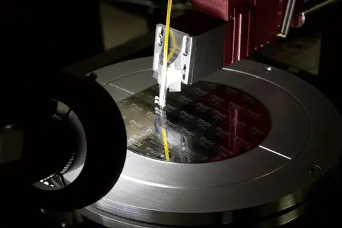
Why switch loss matters
Photonic quantum computers use photons to carry quantum information between components. Switches steer that light along different paths as the system operates. Each switch adds some optical loss: a portion of the signal does not make it through the component. As a system uses more optical components and routes, losses can accumulate and leave fewer photons available for reliable communication between parts of the machine.

In conventional optical links, designers may compensate for a weaker signal by amplifying it. That approach cannot be applied in the same way to quantum information: amplification can disturb or destroy the quantum state being carried by the light. The engineering pressure therefore falls on keeping loss low in the optical path, including at the switching stage.

Insertion loss describes the reduction in signal power introduced when light passes through a component. Xanadu and HyperLight report 7 mdB for their switch, compared with 20 mdB in the companies’ previous demonstration. That is a reduction of 13 mdB in the reported figure. The result is a component-level measurement; by itself, it does not establish the total loss of a complete quantum computer or quantify a system-level improvement in qubit count or reliability.
TFLN platform and manufacturing context
The switch uses thin-film lithium niobate (TFLN) technology and was demonstrated on HyperLight’s TFLN Chiplet platform. The companies say the work used a high-volume wafer manufacturing line. That manufacturing context matters alongside the optical result: a low-loss device has greater practical relevance if the process can reproduce it beyond an isolated laboratory prototype.

Still, the reported demonstration leaves several details open. It does not give the switch’s operating wavelength, bandwidth, switching speed, dimensions, yield, or the test conditions used to measure insertion loss. Those figures would help engineers compare the device with components intended for particular optical architectures and estimate how it might fit into a larger system. The result should be read as a reported switch milestone, not a complete specification sheet.

Using a wafer line also gives the demonstration a different emphasis from a result limited to a single bespoke device. For a component intended for larger systems, repeatable fabrication and integration can affect both the number of usable parts and the effort needed to assemble and test them. The source provides no yield or cost data, however, so the manufacturing implications remain a stated expectation rather than a measured outcome.
From component result to system design
Xanadu founder and chief executive officer Dr Christian Weedbrook described the loss figure as a step toward ramping the switches to production. He said reducing optical loss is one of the key factors for fault-tolerant photonic quantum computing and argued that the lower-loss result could reduce system overhead. These are the company’s expectations; the demonstration does not report a completed fault-tolerant system or a quantified reduction in its resource requirements.
In a large optical architecture, lower loss at each routing point could help preserve more of the signal as it travels between components. That may ease design constraints around how many switches a path can include and how optical resources are allocated. The size of any system-level benefit will depend on the full optical path, including other sources of loss, and on how the switches are arranged and operated.
Weedbrook also said Xanadu expects the advance to improve manufacturing economics and reduce footprint, and pointed to possible value for data centres as they handle faster, more energy-intensive workloads. No measurements for cost, footprint, data-centre performance, or energy use were provided. Those applications remain prospective, and the reported quantum-computing result does not establish performance in data-centre equipment.
The useful next evidence will be how consistently the 7 mdB result holds across devices from the wafer process, alongside fuller operating specifications and integration results. For engineers assessing photonic hardware, the demonstration is a meaningful reduction from the companies’ 2025 figure, while system performance will depend on whether that lower loss carries through manufacturing and into complete optical networks.
 AMD Venice Uses 2.5D Packaging to Feed More Bandwidth Into EPYC Zen 6
 CNC Controller Board Design: Interfaces, PCB Specs and Assembly Testing
 Stratasys and Nano Dimension End $42.5 Million Markforged Sale Agreement